What are the manufacturing processes of the latest integrated circuit engineering?
What are the Manufacturing Processes of the Latest Integrated Circuit Engineering?

I. Introduction
Integrated Circuits (ICs) are the backbone of modern electronic devices, enabling everything from smartphones to supercomputers. These tiny chips, which can contain millions or even billions of transistors, have revolutionized technology and continue to evolve at a rapid pace. The manufacturing processes behind ICs have also advanced significantly, driven by the demand for higher performance, lower power consumption, and miniaturization. This blog post will explore the latest manufacturing processes in integrated circuit engineering, providing insights into the intricate world of semiconductor fabrication.
II. Overview of Integrated Circuit Design
A. Conceptualization and Design
The journey of an integrated circuit begins with its design. Engineers utilize Electronic Design Automation (EDA) tools to create complex circuit layouts. These tools allow for simulation and verification of the circuit's functionality before it is physically manufactured. Design for Manufacturability (DFM) principles are also applied to ensure that the design can be efficiently produced, minimizing potential issues during fabrication.
B. Types of Integrated Circuits
Integrated circuits can be categorized into several types, including:
1. **Analog vs. Digital ICs**: Analog ICs process continuous signals, while digital ICs handle discrete signals. Each type has its specific applications, from audio amplifiers to microprocessors.
2. **Application-Specific Integrated Circuits (ASICs)**: These are custom-designed for a particular application, offering optimized performance for specific tasks.
3. **System on Chip (SoC)**: An SoC integrates all components of a computer or other electronic system onto a single chip, including the CPU, memory, and input/output interfaces.
III. Key Manufacturing Processes
A. Wafer Fabrication
The heart of IC manufacturing lies in wafer fabrication, which involves several critical steps:
1. **Silicon Wafer Production**: The process begins with the production of silicon wafers. Silicon is extracted from quartz sand and purified. Two common methods for crystal growth are the Czochralski and Float Zone methods, which produce high-purity silicon crystals. These crystals are then sliced into thin wafers and polished to achieve a smooth surface.
2. **Photolithography**: This process is essential for defining the intricate patterns on the silicon wafer. A photoresist material is applied to the wafer, and a mask is used to expose specific areas to ultraviolet light. The exposed areas are then developed, revealing the patterns that will guide subsequent etching processes.
3. **Ion Implantation**: To create the necessary electrical properties in the silicon, ion implantation is used to dope the material with impurities. This process involves bombarding the wafer with ions, followed by activation annealing to repair damage and activate the dopants.
4. **Chemical Vapor Deposition (CVD)**: CVD is employed to deposit thin films of materials onto the wafer. There are various types of CVD, including Plasma-Enhanced CVD (PECVD) and Low-Pressure CVD (LPCVD), each suited for different applications in IC manufacturing.
5. **Physical Vapor Deposition (PVD)**: PVD techniques, such as sputtering and evaporation, are used to deposit metal layers on the wafer. These thin films are crucial for creating interconnections between transistors.
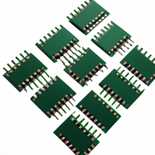
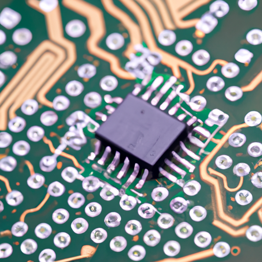
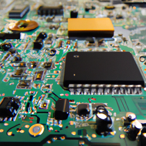
B. Packaging
Once the wafer fabrication is complete, the next step is packaging, which protects the IC and facilitates its integration into electronic devices.
1. **Types of IC Packaging**: There are several packaging options, including:
- **Dual In-line Package (DIP)**: A traditional package with two rows of pins.
- **Surface Mount Technology (SMT)**: A modern approach where components are mounted directly onto the surface of the PCB.
- **Ball Grid Array (BGA)**: A package with an array of solder balls on the bottom, allowing for high-density connections.
2. **Packaging Processes**: The packaging process involves several steps:
- **Die Attachment**: The individual dies are attached to the package substrate.
- **Wire Bonding and Flip-Chip Bonding**: Electrical connections are made using fine wires or by flipping the die and connecting it directly to the substrate.
- **Encapsulation and Sealing**: The package is sealed to protect the IC from environmental factors.
C. Testing and Quality Assurance
Testing is a critical phase in the manufacturing process to ensure the reliability and functionality of the ICs.
1. **Wafer Testing**: Before packaging, individual dies are tested for electrical performance and parametric characteristics. This step helps identify defective chips early in the process.
2. **Final Testing**: After packaging, ICs undergo functional testing to verify their operation. Burn-in testing is also performed to assess reliability under stress conditions, ensuring that only high-quality products reach the market.
IV. Advanced Manufacturing Techniques
As technology advances, so do the manufacturing techniques used in IC production.
A. FinFET Technology
FinFET (Fin Field-Effect Transistor) technology represents a significant leap in transistor design. Unlike traditional planar transistors, FinFETs have a three-dimensional structure that allows for better control of the channel, reducing leakage current and improving performance. This technology is crucial for scaling down transistors to smaller nodes, enabling higher density and lower power consumption.
B. Extreme Ultraviolet (EUV) Lithography
EUV lithography is a cutting-edge technique that uses extremely short wavelengths of light to create smaller features on silicon wafers. This technology allows for the production of ICs with feature sizes below 7 nanometers, pushing the limits of Moore's Law. EUV lithography is essential for the next generation of high-performance chips.
C. 3D IC Technology
3D IC technology involves stacking multiple layers of integrated circuits vertically, allowing for higher density and improved performance. This approach reduces the distance between components, leading to faster communication and lower power consumption. However, it also presents challenges in thermal management and manufacturing complexity.
V. Future Trends in IC Manufacturing
The future of IC manufacturing is shaped by several emerging trends.
A. Emerging Materials
New materials, such as graphene and other 2D materials, are being explored for their potential to enhance performance and reduce power consumption. Silicon carbide (SiC) and gallium nitride (GaN) are also gaining traction for high-power and high-frequency applications.
B. Sustainability in IC Manufacturing
As environmental concerns grow, the semiconductor industry is focusing on sustainability. Energy-efficient manufacturing processes and waste reduction initiatives are becoming priorities, with companies seeking to minimize their environmental footprint.
C. Automation and Industry 4.0
The integration of AI and machine learning in manufacturing processes is revolutionizing the industry. Smart factories equipped with IoT devices enable real-time monitoring and optimization of production, leading to increased efficiency and reduced costs.
VI. Conclusion
The manufacturing processes of integrated circuits are complex and continually evolving. From wafer fabrication to advanced packaging and testing, each step is crucial in producing high-quality ICs that power our modern world. As technology advances, new materials and techniques will further enhance the capabilities of integrated circuits, ensuring their relevance in an ever-changing technological landscape. The future of IC manufacturing promises exciting innovations that will continue to shape the way we live and work.
VII. References
1. Academic journals and articles on semiconductor manufacturing.
2. Industry reports and white papers from leading semiconductor companies.
3. Books on integrated circuit design and manufacturing processes.
This blog post provides a comprehensive overview of the latest manufacturing processes in integrated circuit engineering, highlighting the intricate steps involved in bringing these essential components to life.